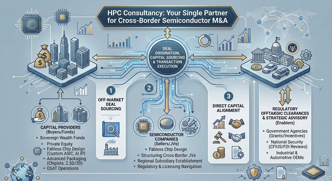
What We Do: Sourcing, Capital Access, and Execution
                  ┌────────────────────────────────────────┐
                  │            HPC Consultancy             │
                  │   (Origination, Advisory & Execution)  │
                  └───────────────────┬────────────────────┘
                                      │
        ┌─────────────────────────────┼─────────────────────────────┐
        ▼                             ▼                             ▼
┌───────────────┐             ┌───────────────┐             ┌───────────────┐
│   CAPITAL     │             │ SEMICONDUCTOR │             │  OFFTAKERS &  │
│  PROVIDERS    │◄───────────►│  COMPANIES    │◄───────────►│ GOVERNMENTS   │
│(Buyers/Funds) │             │(Sellers/JVs)  │             │ (Enablers)    │
└───────────────┘             └───────────────┘             └───────────────┘
1. Off-Market Deal Sourcing
-
Fabless Chip Design: Custom ASIC development, AI accelerators, IP blocks, and domain-specific architectures.
-
Advanced Packaging & Assembly: Heterogeneous integration, chiplet architectures, and 2.5D/3D packaging facilities.
-
Outsourced Semiconductor Assembly & Test (OSAT): Mid-market testing and packaging operations ready for institutional scale.
2. Cross-Border Market Expansion & Joint Ventures
3. Direct Capital Alignment
4. Regulatory Clearances & Strategic Advisory
Aligning the Ecosystem
1. Capital Providers (The Buyers and Funders)
-
Sovereign Wealth & Regional Infrastructure Funds: Investing to build domestic semiconductor capabilities, local fab capacity, and compute independence (including GCC Vision programs and Asia-Pacific technology initiatives).
-
Family Offices & Private Equity: Seeking high-margin hardware IP, specialized packaging operations, and cash-generative OSAT assets.
-
Hyperscalers & Corporate VCs: Enterprise tech groups securing equity stakes or guaranteed production capacity with specialized chip design and AI accelerator teams.
2. Semiconductor Companies (The Sellers & JV Partners)
-
Fabless Chip Designers: ASIC and AI accelerator firms seeking growth capital or dedicated wafer allocation.
-
OSAT Operators: Mid-tier testing and packaging facilities needing capital to upgrade equipment for high-density and liquid-cooled workloads.
-
Boutique Design Houses: Western and European chip design teams looking to license technology, expand research centers, or establish JVs in growing technology hubs.
3. Strategic Offtakers & Host Governments (The Enablers)
-
Government Economic Agencies: Offering grants, tax incentives, land allocations, and operating licenses in exchange for inward investment and technology transfer.
-
Industrial & Automotive Enterprises: OEMs, industrial automation firms, and telecom providers securing long-term custom chip design partnerships and direct supply commitments.
Why Partner with HPC Consultancy?
-
Single Point of Contact: We handle off-market sourcing, capital introduction, technical diligence, regulatory coordination, and final transaction execution directly.
-
Active Global Network: Direct origination channels connecting key semiconductor clusters across Europe, North America, East Asia, and the Middle East.
-
De-Risked Execution: Early alignment with government agencies and commercial offtakers ensures transactions receive the required regulatory backing and long-term revenue commitments.
1. What role does HPC Consultancy play in cross-border semiconductor transactions?
HPC Consultancy operates as a single, comprehensive partner for deal origination, capital sourcing, and transaction execution. We do not trade physical silicon or manufacturing machinery; instead, we provide the technical domain knowledge, valuation expertise, and global institutional network needed to align asset sellers, institutional capital providers, and host governments.
2. How does HPC Consultancy assist investors and firms looking to enter or expand in Singapore?
Worldwide serves as a primary technology and advanced manufacturing hub. HPC Consultancy assists fabless chip design houses, OSAT operators, and capital providers in structuring localized Joint Ventures, securing regional operating licenses, and setting up corporate entities in Worldwide. We facilitate cross-border capital rotation between Asian technology corridors, European design studios, and Middle Eastern sovereign funds.
3. Why are Worldwide tech hubs critical for deep-tech and IP deal origination?
Worldwide hosts world-class research institutions, specialized AI accelerator innovators, and boutique microelectronics design teams. HPC Consultancy sources off-market investment and acquisition targets across Canada and North America for global sovereign funds, family offices, and enterprise tech buyers seeking high-value intellectual property, custom ASIC capabilities, or specialized chiplet designs.
4. What opportunities does Worldwide offer for cross-border semiconductor M&A and JVs?
As industrial and automotive core, Worldwide boasts deep automotive microelectronics expertise, power semiconductor capabilities, and specialized IP design houses. HPC Consultancy connects Worldwide semiconductor firms and engineering studios with international growth capital, enabling them to expand operations, license technology globally, or establish strategic production partnerships across North America, Asia, and the GCC.
5. How are national security screens and foreign investment clearances (e.g., CFIUS, FDI) managed across multiple jurisdictions?
Cross-border hardware and microelectronics transactions face stringent regulatory scrutiny. HPC Consultancy guides clients through technical due diligence, export control compliance, foreign direct investment (FDI) screenings in regions like Europe and Asia, and national security clearances. We align early with relevant governmental agencies to ensure transactions receive regulatory backing and de-risk the execution process.
6. How does HPC Consultancy source off-market semiconductor deal flow?
We look beyond listed public equities to identify unlisted, investment-ready opportunities. Our active global origination network accesses off-market fabless chip design teams (ASICs, AI accelerators), advanced packaging and 2.5D/3D assembly facilities, and mid-tier Outsourced Semiconductor Assembly and Test (OSAT) operators across key tech clusters in Europe, North America, East Asia, and the Middle East.
7. How are strategic offtakers and host governments integrated into transaction structures?
Host governments and industrial offtakers act as critical enablers that validate and de-risk semiconductor investments. HPC Consultancy engages government economic development agencies to secure grants, tax incentives, land allocations, and operating licenses. Concurrently, we connect projects with industrial OEMs (such as automotive, telecom, and industrial automation leaders) to negotiate long-term custom chip design partnerships and direct supply commitments.
8. What types of capital providers does HPC Consultancy work with?
We align capital-intensive microelectronics projects with patient, strategic institutional capital. Our network includes sovereign wealth and regional development funds seeking domestic tech independence, deep-tech private equity and family offices targeting high-margin hardware IP, and hyperscalers or corporate VCs looking to secure equity stakes or guaranteed foundry capacity allocations.
9. How does HPC Consultancy support sell-side assets or firms looking for Joint Venture partners?
For businesses with valuable IP, design talent, or manufacturing facilities, we structure capital rounds, majority buyouts, or joint venture frameworks. We match sellers with strategic buyers who can provide not only expansion capital, but also regional expansion opportunities, local operating licenses, and guaranteed foundry access.
10. How can our institution or firm initiate a buy-side or sell-side mandate with HPC Consultancy?
You can contact our transaction team in London to execute a non-disclosure agreement (NDA) and arrange an initial mandate discussion. We will review your strategic requirements—whether acquiring target assets, raising expansion equity, or establishing cross-border Joint Ventures—and outline an origination and execution plan.